|
|
|
||||||||||||||||||||


|
|||||||||||||||||||


 물품구매안내")


 톡톡
톡톡- 이 브레드 보드 호환 모듈은 부피가 큰 전원 스위치의 대안입니다. 이것은 주위의 연속 흐름을 제공 할 수있는 하이 사이드 전원 MOSFET 제어 작은 집적 슬라이드 스위치를 사용하여 도 8a 에 40 V로 4.5 V를 . 이 보드는 역 전압 보호 기능을 갖추고 있으며 외부 스위치 또는 마이크로 컨트롤러의 디지털 출력으로 MOSFET을 쉽게 제어 할 수 있습니다.
-
[로봇사이언스몰][Polou][폴로루] Big MOSFET Slide Switch with Reverse Voltage Protection, MP #2814
상품번호 : 16199 아이콘 설명보기
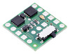
![[로봇사이언스몰][로봇사이언스몰][Polou][폴로루] Big MOSFET Slide Switch with Reverse Voltage Protection, MP #2814>>이 브레드 보드 호환 모듈은 부피가 큰 전원 스위치의 대안입니다. 이것은 주위의 연속 흐름을 제공 할 수있는 하이 사이드 전원 MOSFET 제어 작은 집적 슬라이드 스위치를 사용하여 도 8a 에 40 V로 4.5 V를 . 이 보드는 역 전압 보호 기능을 갖추고 있으며 외부 스위치 또는 마이크로 컨트롤러의 디지털 출력으로 MOSFET을 쉽게 제어 할 수 있습니다.](/data/goods/1/2021/02/16199_temp_16127624381617view.jpg)
This breadboard-compatible module is an alternative to bulky power switches. It uses a small integrated slide switch to control a high-side power MOSFET that can deliver continuous currents up to around 8 A at 4.5 V to 40 V. The board features reverse-voltage protection and also makes it easy to control the MOSFET with an external switch or the digital output of a microcontroller.
 Compare all products in Pololu Power Switches.
Description
Overview

This product is a power switch implemented as a pair of P-channel MOSFETs configured as a high-side switch with reverse voltage protection and controlled by a micro slide switch. Because the main current does not go through the controlling mechanical switch, a variety of switches can be used without concern for the current they can carry. For example, a small slide or toggle switch can be mounted conveniently on a control panel with thin wires running to it, while the main power path can be shorter and with thicker wires. Pushbutton or tactile switches can also be used for momentary switching applications.
Unlike the Pololu Pushbutton Power Switches, which can lose their state when power is disconnected and reapplied, the conducting state of the MOSFET Slide Switches is determined only by the physical control switch (or a signal supplied to the “ON” pin), independent of power applied to the board. This can make them more appropriate for applications where the supplied power may be intermittent.
Warning: Do not use this switch as an emergency cutoff or similar safety disconnect in applications where failure to cut power could lead to injury or property damage.
Four versions of the MOSFET slide switches are available:
The two Mini MOSFET Slide Switches are smaller, lower-current versions that are useful for applications with tight size constraints or lower power requirements. Also, the the Mini LV is the only one of the four that works below 4.5 V; since it can operate down to 1.8 V, this version can be used with a single lithium cell battery.

The pinout of the Big version is the same as the pinout of the Mini version with several additional redundant connection points for convenience, including main power connections that are compatible with 5 mm terminal blocks.
The primary functional difference between the each of the units arises from the MOSFET used, which sets the operating range and performance of the units:
 LV | 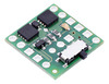 SV | 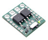 MP | 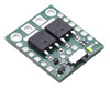 HP | |
|---|---|---|---|---|
| Absolute max voltage: | 20 V | 40 V | ||
| Recommended operating voltage: | 1.8 V to 16 V | 4.5 V to 32 V | ||
| MOSFET combined on resistance (max) | 26 mΩ @ 1.8 V | |||
| 16 mΩ @ 4.5 V | 90 mΩ @ 4.5 V | 40 mΩ @ 4.5 V | 13 mΩ @ 4.5 V | |
| 50 mΩ @ 10 V | 30 mΩ @ 10 V | 8.6 mΩ @ 10 V | ||
| Continuous current at 55°C(1) | 3.0 A | 2.0 A | 4.0 A | 6.0 A |
| Continuous current at 150°C(1) | 6.0 A | 4.3 A | 8.0 A | 16 A |
| Maximum current | 12 A | 7.2 A | 40 A | 90 A |
| Current consumption in on state(2) | ~210 μA/V | ~65 μA/V | ||
| LED color | red | green | ||
| Size | 0.6″ × 0.6″ × 0.1″ | 0.8″ × 1.0″ × 0.16″ | ||
| Weight | 0.6 g | 2.7 g | ||
1 At 12 V with ambient temperature of 22°C in still air.
2 On state current is dominated by indicator LED; current is approximately proportional to input voltage.
Using the MOSFET Slide Switch


If the physical switch is in the “off” position, the switch state can also be controlled by a digital signal (e.g. from a microcontroller) via the “ON” control pin. Driving the “ON” pin low (or leaving it disconnected) will leave the switch off; driving the pin beyond approximately 1 V will turn the switch on. The maximum voltage for the “ON” pin is 30 V, independent of the switch voltage (VIN).
Each power node can be accessed through a large hole along the top side of the board or two smaller 0.1″-spaced holes along the sides of the board. For applications drawing more than 5 A, you should either use the large holes or both 0.1″-spaced holes for each power connection.
Included Hardware


Two 6-pin straight breakaway male headers and two 2-pin 5mm terminal blocks are included with each switch, and you can choose which of these components, if any, to solder to the board. The terminal blocks work with the four large holes, and the header strips allow the switch to be used with solderless breadboards and perforated circuit boards with standard 0.1″ spacing. If you want to use the terminal blocks, we recommend you install them on the side of the board without components, as shown in the above breadboard picture. The terminal blocks will cover one of each of the smaller VIN and VOUT holes, so you should not solder header pins into those holes if you plan on using terminal blocks.
Note that the terminal blocks are only rated for 16 A, so for higher-power applications, thick wires should be soldered directly to the board.

Thermal and power dissipation considerations
Because MOSFETs in the on state are effectively resistive, the power heating the board is proportional to the square of the current flowing through it. The comparison table near the top of this page shows typical currents that heat the MOSFETs to 55°C, where the MOSFETs start being noticeably warm but are still generally safe to touch, and currents that heat the MOSFETs to 150°C the absolute limit for the MOSFETs. With adequate cooling, or for brief periods if the MOSFETs are not hot to begin with, currents up to the listed maximums are attainable.
Transient protection
Interrupting large currents can cause voltage spikes (positive on the input side and negative on the output side) that depend on the inductance of the power connections and that can exceed the limits of the device. Appropriate measures to limit the size of these spikes include minimizing lengths of wires, placing capacitors at the power switch to smooth the spikes and absorb some of the energy, placing a schottky diode across the power output to absorb negative spikes, and placing a transient voltage suppressor (TVS) across the power input to absorb positive spikes.
Schematic diagram

Dimensions
| Size: | 0.8″ × 0.9″ × 0.16″1 |
|---|---|
| Weight: | 2.6 g2 |
General specifications
| Current rating: | 8 A3 |
|---|---|
| Minimum operating voltage: | 4.5 V |
| Maximum operating voltage: | 40 V4 |
| Reverse voltage protection?: | Y |
Identifying markings
| PCB dev codes: | psw04b |
|---|---|
| Other PCB markings: | 0J9260 |
Notes:
- 1
- Without included optional connectors. This also does not include the slide switch lever, which extends past the edge of the board by approximately 0.04″ (1 mm).
- 2
- Without included optional connectors.
- 3
- Continuous at 12 V, without exceeding 150°C.
- 4
- Recommended maximum is 32 V.
File downloads
 아이콘이 부착된 상품
 b. 해외상품 :
1) 해당상품:  아이콘이 부착된 상품
2) 구매금액 700,000원 이상 : 입금확인 후 최소 5일 ~ 최대 2주
3) 구매금액 700,000원 이하 : 입금확인 후 최소 1주 ~ 최대 8주
4) 단, 해외계약업체에 품절되지 않은 상품에 한함
② 구매상품 종류가 많을 경우 예상 준비기간 보다 더 소요 될 수 있습니다.
③ 주문하신 상품은 출고완료 메일 또는 문자 수신 후 익일~최대7일(도서,산간지역)
이내에 수령하실 수 있습니다.
④ 제주(\3,500원)/도서지역(\5,000원)은 배송비가 추가됩니다.
제주,도서, 산간지역은 타 지역보다 배송기간이 길어질 수 있습니다.
⑤  아이콘이 부착된 상품이라도 국내재고가 있을 수 있습니다.
⑥ 해외 현지 사정으로 인해 공지한 배송기간보다 더 길어 질 수 있습니다.
⑦ 해외상품은 반품/교환/취소가 어려울 수 있으니 신중히 주문하시기 바랍니다.
3. 소비자의 단순변심/착오구매에 의한 청약철회제한안내
① 전자상거래 등에서의 소비자보호에 관한 법률 제17조 제2항 및 동 시행령
제21조에 의한 청약철회 제한 사유에 해당하는 경우 및 기타 객관적으로
이에 준하는 것으로 인정되는 경우에 한합니다.
② 소비자의 단순변심, 착오구매에 의한 교환/반품 시에 발생하는 배송비는
소비자가 부담합니다.
③ 판매자의 실수,제품하자 등의 사유로 인한 배송비는 판매자가 부담합니다.
4. 상품의 교환/반품/보증조건 및 품질보증기준안내
① 상품이 공급된 날(배송완료일)로부터 7일 이내에 교환/반품을 신청 할 수 있습니다.
그러나 아래의 사유에 해당 하는 경우에는 교환/반품 신청이 받아들여지지 않을 수도 있습니다.
a. 소비자의 책임으로 인해 상품이 훼손/멸실 된 경우(확인을 위한 포장훼손제외)
b. 소비자의 사용에 의해 상품의 가치가 현저하게 감소한 경우
c. 시간의 경과로 인해 상품의 재판매가 불가하게 된 경우
d. 판매방식의 특성으로 판매자에게 회복할 수 없는 피해가 발생한 경우 (주문제작 상품, 청약철회상품 등)
② 교환/반품/보증조건 및 품질보증기준은 『소비자기본법』에 따른 소비자분쟁해결기준에 따라 피해를 보상합니다.
5. 소비자피해보상 처리, 재화 등에 대한 불만 및 분쟁처리 안내
관련상품
-
![[로봇사이언스몰] 메이커스: 어른의 과학 Vol.06 이공계 연구소 보드게임](/data/goods/1/2022/10/20106_temp_16655616023677view.png)


- [로봇사이언스몰] 메이커스: 어른의 과학 Vol.06 이공계 연구소 보드게임
- 이과생 마음 두근거리게 하는, 과학자가 만든 과학자 되어보기 보드게임
- 판매가 ₩ 78,000
-
 1,458
1,458
-
- 조건부 무료배송
-
![[로봇사이언스몰][코딩로봇] 알파 미니 (ALPHA MINI)](/data/goods/1/2020/06/15334_tmp_32a415fdf174c952317188293d01b0684901view.jpg)
- [로봇사이언스몰][코딩로봇] 알파 미니 (ALPHA MINI)
- 로봇을 활용한 재미있는 코딩학습
- 판매가 ₩ 1,250,000
-
9,999+
-
- 조건부 무료배송
-
- 아두이노 우노 R3 고급 키트
- 아두이노 실습을 위한 필수 부품이 포함된 키트, 아두이노 코딩 배우기 교재가 제외된 상품입니다.
- 판매가 ₩ 65,340
-
6,707
-
- 조건부 무료배송
-
![[로봇사이언스몰][블루이노] 스마트팜 인공지능 키트](/data/goods/1/2021/05/17457_temp_16218314494856view.png)
- [로봇사이언스몰][블루이노] 스마트팜 인공지능 키트
- 인공지능이 가미 된 내가 직접 스마트팜을 구축하고 식물을 키워볼 수 있는 키트입니다.
- 판매가 ₩ 638,000
-
9,999+
-
- 조건부 무료배송
판매자 관련상품
-
- [로봇사이언스몰][코딩로봇] 알파 미니 (ALPHA MINI)
- 로봇을 활용한 재미있는 코딩학습
- 판매가 ₩ 1,250,000
-
9,999+
-
- 조건부 무료배송
-
- [로봇사이언스몰] 메이커스: 어른의 과학 Vol.06 이공계 연구소 보드게임
- 이과생 마음 두근거리게 하는, 과학자가 만든 과학자 되어보기 보드게임
- 판매가 ₩ 78,000
-
1,458
-
- 조건부 무료배송
-
- [로봇사이언스몰][블루이노] 스마트팜 인공지능 키트
- 인공지능이 가미 된 내가 직접 스마트팜을 구축하고 식물을 키워볼 수 있는 키트입니다.
- 판매가 ₩ 638,000
-
9,999+
-
- 조건부 무료배송
-
![[로봇사이언스몰][교육용드론][CoDrone] 코드론 미니](/data/goods/1/2020/01/14879_tmp_f6cf2ca48125c96d1f029e73a51f1bd87855view.png)
- [로봇사이언스몰][교육용드론][CoDrone] 코드론 미니
- 코딩이 가능한 미니드론/안정적 군집 비행 3대
- 판매가 ₩ 99,000
-
9,999+
-
- 조건부 무료배송
판매자 정보
| 판매자 | 본사 | 셀러등급 | |
|---|---|---|---|
| 상호명 | (주)위키모바일(로봇사이언스몰) | 대표자 | 김경식 |
| 사업자등록번호 | 215-87-14086 | 통신판매신고번호 | 제2008-서울송파-0867호 |
| 연락처 | 02-2283-1300 | 사업장 소재지 | 서울특별시 송파구 문정동 643-1 엠스테이트 B동704호 |
2. 해외구매 특성상 주문에서 배송까지는 평균 10~15일이 소요됩니다. 간혹 현지 제품 수급에 따라 부득이하게 시일이 더 소요 될 수 있으니 구매시 좀 더 여유있게 주문하시길 권합니다.
3. 해외 내수품인 관계로 A/S에 대해서는 별도의 책임을 지지 않습니다.
4. 해외배송 특성상 주문접수후 배송상태가 배송준비중으로 넘어간 경우 해외에서 국내로의 배송이 이루어지고 있다는 뜻입니다. 따라서 배송준비중으로 배송상태가 넘어간 경우 취소및 반품이 불가하므로 이점 양해 부탁드립니다.
5. 타 해외구매대행 사이트에서 주문하신 물건과 주문날짜가 겹치지않도록 주의해 주십시오. 통관날짜가 같을 경우 합산관세가 부가되게 됩니다.